产品动态 · 2026-06-05

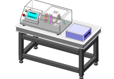
Photonic integration is the key to extending Moore's Law, and the refractive index, thickness, and loss of optical waveguide thin films directly determine the performance and yield of photonic chips. Shanghai Yanrun's high-precision prism coupler, based on total internal reflection and evanescent-wave coupling, accurately measures thin-film optical parameters for photonic chip R&D, process monitoring, and quality inspection.
Technical Breakthroughs
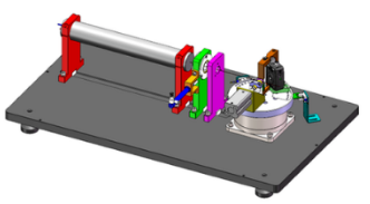
Authoritative principle: Based on attenuated total reflection (ATR) and the optical tunneling effect, the instrument obtains the effective refractive index of waveguides by scanning the resonance angle. It is the industry's recognized gold standard for thin-film optical parameter measurement, capable of characterizing single-layer and multi-layer films on all kinds of wafers and substrates.
Top-tier accuracy: Equipped with a high-precision air-bearing rotary stage and a closed-loop control system, it delivers an angular resolution of 0.001° and repeatability better than ±0.002°, capturing even weak resonance dips. Refractive index measurement accuracy reaches ±0.001, and film thickness measurement accuracy reaches up to ±1 nm (depending on film type and thickness), meeting advanced international standards.
Fully self-developed and controllable: The instrument hardware, control system, and core solving algorithms are all independently developed, forming a complete technical system from theoretical modeling and simulation optimization to experimental verification. Customized function upgrades and local data processing are supported, ensuring R&D data security and full autonomy over the measurement workflow.
Broad Market Prospects
With the rapid growth of silicon photonics, LiDAR, and high-speed optical communications, industry demand for in-line monitoring of thin-film optical parameters and closed-loop process control keeps rising. The instrument covers high-precision measurement needs across the entire cycle from R&D and tape-out to mass production, ensuring consistent yield and performance. Its modular design also adapts to precision inspection in semiconductors, displays, optical coating, and other fields, making it core equipment for domestic breakthroughs and production ramp-up in high-end optoelectronic products.
Published by MICROCRE. Please credit when sharing.
Back to news ←